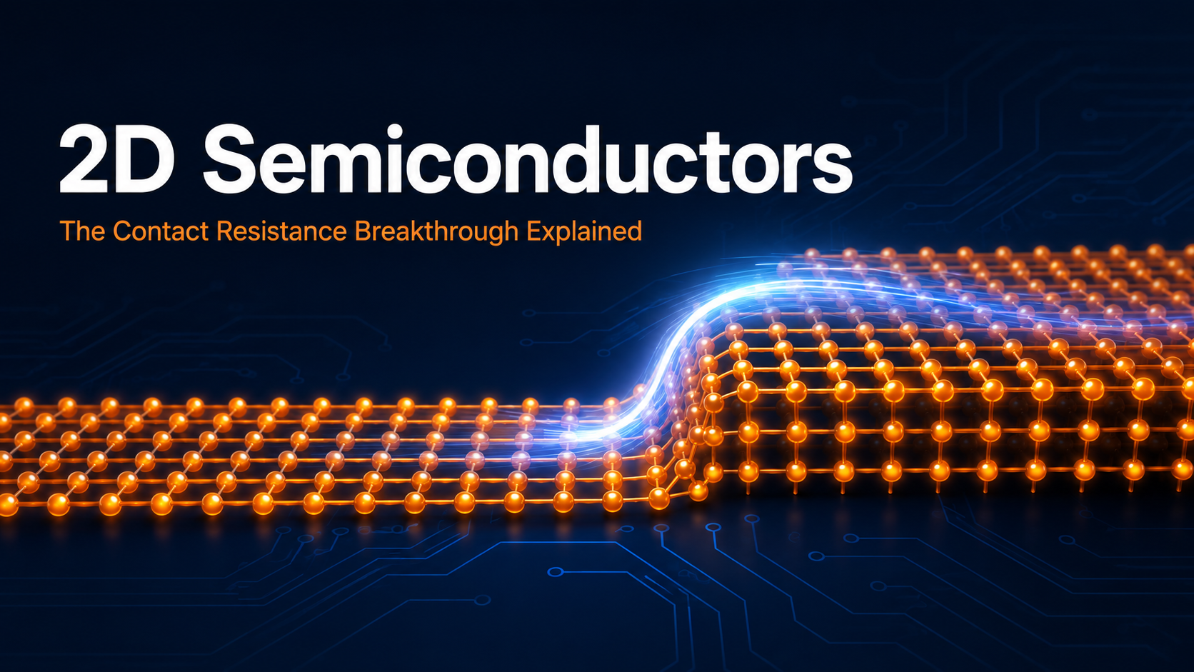
2D semiconductors are materials just one or a few atoms thick that can carry out the same switching work as the silicon in today's chips, and they are the industry's leading candidate for keeping transistor scaling alive once silicon runs out of room. In June 2026, researchers at KAIST in South Korea removed one of the biggest obstacles standing in their way: they showed that a single sheet of platinum diselenide (PtSe2) can act as both the electrical contact and the semiconductor, letting current flow across the junction without the resistance penalty that normally appears where a metal touches a chip. Here is what they actually demonstrated, and what it does and does not mean for anyone who buys electronic components for a living.
The problem: the resistor nobody designs in
Every transistor needs metal electrodes to get current in and out. At the boundary where metal meets semiconductor, charge carriers hit a barrier, and the result is contact resistance: wasted power, extra heat, and a hard ceiling on how much benefit each new round of miniaturisation can deliver. As transistors have shrunk, this parasitic resistance has grown into one of the dominant loss terms in advanced chips. For atomically thin 2D materials the problem is worse still, because pressing a metal electrode onto a sheet a few atoms thick tends to damage or chemically alter the very layer it is supposed to feed.
What the KAIST team actually did
The team led by Professor Seungbum Hong of KAIST's Department of Materials Science and Engineering, working with Professor Kibum Kang and Professor Sung Beom Cho of Sungkyunkwan University, sidestepped the metal electrode entirely. PtSe2 has a useful quirk: its electronic character depends on how thick the film is. Thicker regions behave like a semimetal, conducting freely; thinner regions behave like a semiconductor. By forming thick and thin regions within one continuous film, the researchers built a conductor and a semiconductor out of the same crystal, joined without any physical break. There is no foreign interface for charge to fight through.
The evidence is what makes the paper notable. Using atomic force microscopy combined with in-plane current detection, the team mapped charge movement across the boundary at nanometre scale and showed the current passing from the semimetallic region into the semiconducting region without being blocked or deflected. They also gated the semiconducting region and switched the current on and off, confirming the structure can do real transistor work, not just conduct. The results were published in the journal Matter under the title "Nanoscale imaging of charge transport across the semimetal-semiconductor interface in monolithic platinum diselenide."
The honest caveats
The researchers themselves are clear about what remains unsolved: reliability, circuit-level integration and large-scale manufacturing. Growing a wafer-sized film with atomically precise thickness steps, repeatably, in volume, is a different order of problem from demonstrating one beautiful interface under a microscope. This is a genuine advance in understanding, not a product announcement.
How long before this reaches a BOM?
History gives a sober calibration. The FinFET transistor was demonstrated in university labs around the turn of the millennium and reached volume production at Intel in 2011, roughly a decade later. EUV lithography took about two decades from serious research to high-volume manufacturing in 2019. Wide-bandgap materials like SiC and GaN spent even longer maturing from papers into the power components now on the shelf. Industry roadmaps place 2D-material channels in the 2030s, and results like KAIST's are exactly the kind of groundwork those roadmaps depend on. If your products ship this decade, nothing on your bill of materials changes because of this paper.
Why component buyers should still pay attention
Breakthroughs like this one matter to procurement for a different reason: they show where the industry's capital and fab capacity will migrate next. Every major technology transition pulls investment toward the new architecture and quietly starves the old one, and buyers live in the aftermath. We are watching that mechanism right now as AI demand redirects memory capacity away from mainstream DRAM, and as mature parts across the market drift toward end of life while manufacturers refocus on newer nodes. When 2D semiconductors eventually take their place in leading-edge logic, the same wave will roll through again: silicon designs will not disappear, but the parts your long-lifecycle products depend on will get less attention, longer lead times and earlier obsolescence notices. The buyers who fare best in every transition are the ones who track lifecycle status early and secure supply before the squeeze, a discipline we cover in our guide for European OEMs navigating the 2026 shortage.
How GlobX helps
GlobX is an independent electronic-component distributor in Neu-Isenburg, Germany. While the research world works on the chips of the 2030s, we keep the chips of the last three decades flowing: hard-to-find, obsolete and allocated parts sourced through a verified global supplier network, with ISO 9001 incoming inspection, anti-counterfeit checks and full traceability. Browse our component catalog or request a quote; we respond within 24 hours.